Other articles on FTTP:
Download PDF version of this article
A. F. J. Levi
September 2001.
Fiber-to-the-processor:
A technology convergence point
Driving microprocessor systems to a crisis
Moore’s Law [1] continues to dominate the development of microprocessors. As shown in Fig. 1, the number of transistors per chip doubles every two years. This creates both opportunity and challenges.
During the last decade, CMOS technology has scaled from 1.0 mm to 0.18 mm minimum feature size enabling an increase in the number for transistors per chip from about 1.2 million to 42 million [2]. Over the same period, the associated improvement in transistor performance, greater power consumption and improved architecture has allowed clock rates to increase by 30 times (i486DX – P4) [3]. The increase in number of transistors per chip has provided opportunity for innovation in micro-architecture by, for example, increasing the number of special-function logic blocks, implementing out-of-order speculative execution, deep pipelining and increasing cache size. The combination of increased number of transistors, increased clock rate and improved architecture has dramatically enhanced total microprocessor performance.
Moore’s Law will continue to influence microprocessor design for the present decade until 0.03 mm CMOS technology is implemented. By the year 2010 architectures calling for a billion transistors on a chip operating at clock rates in excess of 10 GHz and delivering nearly a trillion instructions per second will be considered. Multi-threading and multiple-processor architectures on a single-chip will be adopted to increase throughput and the number of operations per second. Unfortunately, these trends will result in dramatically increased power consumption and exert significant bandwidth performance demands at the platform level.
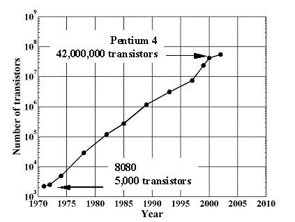
Fig. 1 – Moore’s Law has successfully predicted that the total number of transistors on a microprocessor doubles every two years. [2] |
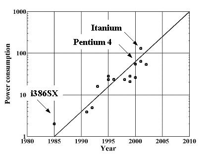
Fig. 2 – Microprocessors power dissipation as a function of year showing extrapolation towards 1 kW by 2010 [3]. |
Power dissipation will become a critical factor in the coming years. As shown in Fig. 2, simple extrapolation of current trends predicts microprocessors with power dissipation approaching 1000 W by 2010. Power consumption at these levels in a single die is not practical. Reduction of power consumption and power management will become a dominant aspect of design. This is a significant challenge that will increasingly preoccupy design effort. System architects will seek solutions from new and emerging technologies to find better system design points. A promising approach is to emphasize high-speed IO and de-emphasize increase in number of transistors per chip.
In the coming years, the imbalance between microprocessor performance and memory access will be driven to a crisis point. As illustrated by Fig. 3, with successive generations, the difference between microprocessor and memory-bus clock rate continues to grow. Without a new approach, the microprocessor will lose hundreds of process cycles while waiting for a single read from main memory. Again, system architects will push electrical bus rates into the GHz range and increase bus widths. Unfortunately, this approach becomes significantly more difficult with increasing clock frequency.
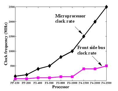
Fig. 3 – The imbalance between microprocessor clock rate and memory bus clock rates continues to grow with successive generations of microprocessor.[3] |
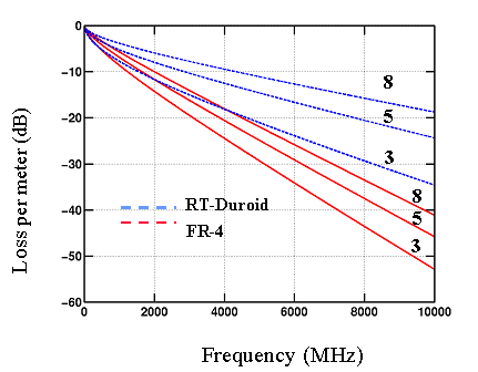
Fig. 4 – Simulated loss per meter for 50 W microstrip including skin-effect and dielectric losses for FR-4 (er= 4.5, tan d = 0.02) and RT-Duroid (er = 2.35, tan d = 0.005) for trace widths 8, 5 and 3 mils in 1 oz copper.[4] |
At high memory-bus frequencies controlled impedance lines are required and this results in increased electrical power consumption. In addition, as illustrated in Fig. 4, losses in micro-strip lines implemented in FR4 increase significantly with frequency. This also impacts power consumption. Another very serious issue that relates to cost-effective packaging is the difficulty in launching high-speed signals. This is illustrated in Fig. 5 where S11 is shown as a function of frequency for a standard high-frequency test fixture. Controlled launch for each signal across a wide bus and maintaining impedance through vias is a major challenge for an all-electronic approach.
The overall trend in microprocessor development is one that is being driven to a crisis in both power dissipation and memory access. Solutions based on conventional electronics and packaging will increasingly fail to effectively remove the stress imposed on system performance. Fiber-optics is the radically different technology which will provide the path forward for future system design. Here, the electronics industry will benefit from the development and maturation of fiber-based telecommunication technologies.
The adoption of fiber-optic technologies for communication
Since the invention of the laser in 1958 there has been interest in applying it to communications. The first installation of a fiber-optic telephone link was in 1977. It took a few more years before the first transcontinental fiber-optic telephone link (TAT-8) was installed in 1988. Today, Wide Area Networks (WANs) based on fiber-optics has permeated every aspect of terrestrial communication. The driving forces behind this rapid adoption are the high data-bandwidth, long-distance transmission at low optical-loss and the relatively low-cost of implementation and upgrade.
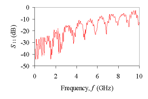
Fig. 5 – Measured S11 as a function of frequency for a standard 50 W high-speed electrical test-fixture (Tektronix #671-3273-00). Inadequacies of the SMA launch onto a 3”-long, 60 mil wide microstrip trace result in severe reflections at 10 GHz.[4] |
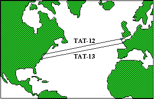
Fig. 6 – TAT 13/14 is a fiber-optic submarine cable WAN that connects the United States to Europe. Brought into service in 1995, it cost $0.75B and has an expected life of 25 years. It is a ring network consisting of two fiber pairs in each cable. Each pair transfers data at 5 Gb/s and the network has a capacity of 300,000 simultaneous voice channels. The total length of the ring is 14,000 km and there are fiber-optic amplifiers every 45 km. |
The success of fiber-optic insertion in telephone systems and the promise of economies of scale from a larger component market resulted in adoption of fiber for Metropolitan Area Networks (MAN) and Local Area Network (LAN) connectivity where low-cost is a dominant factor. The Gigabit Ethernet standard (IEEE 802.3z) of 1998 and the 10 Gigabit Ethernet standard (IEEE 802.3ae) in progress in 2001 are representative of the adoption of fiber-optics for the LAN environment.
The reduction in implementation cost has allowed other optical networks such as Fibre Channel (FC) to link machine-room facilities to remote disk storage.
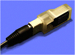
Recently, fiber-optics has been used to solve a different class of problems in machine-room and system interconnect. Here, the difficulty is an edge-connection IO bottleneck at the box-to-box and board-to-board level [5]. In these very short reach applications [6], link distance is less than 300 m, so the advantage of fiber-optics for long-distance transmission is not important. However, electrical interconnects simply fail to provide the needed edge-connection bandwidth density (measured in units of Gb/s/cm) and this is where fiber optics has another distinct advantage. A popular solution is use of parallel fiber-optic transmitter and receiver modules [7] which today provide up to twelve independent links with an edge-connection bandwidth density near 30 Gb/s/cm (3.7 GB/s/cm). A parallel fiber-optic module is shown in Fig. 7. Future, straight-forward scale-up of this technology should achieve bandwidth density of 120 Gb/s/cm (15 GB/s/cm) and adoption of Wavelength Division Multiplexing (WDM) is capable of increasing bandwidth density by an additional factor of ten to deliver 1.2 Tb/s/cm (150 GB/s/cm).
|
Fig. 7– Example of parallel fiber-optic transmitter module using VCSEL technology developed by Agilent [7].The BGA for surface mount to a PCB and the 12 b-wide parallel fiber-optic push-pull connector are clearly visible. Today, such commercially available modules have a bandwidth density of 30 Gb/s/cm |
(a)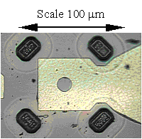 (b) (b)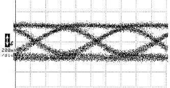
Fig. 8 – (a) Photograph of a typical GaAs/AlGaAs oxide-confined VCSEL viewed from above. The light-emitting area is the small region in the center of the image (b) Transmitted eye-diagram at 2.5 Gb/s of a VCSEL with threshold current 0.5 mAand 1.6 mApp drive current. Horizontal scale is 200 ps/div.[8] |
Key to recent advances in fiber-optic interconnects is the development of efficient, high-speed Vertical Surface Emitting Lasers (VCSELs). Importantly, these devices can consume less power than an equivalent all-electrical LVDS transmitter.
It is the remarkable bandwidth density scaling, the use of power-efficient vertical-cavity surface-emitting lasers (VCSELs), low-cost interface electronics, and inexpensive packaging that make fiber-optics so attractive for addressing the needs of microprocessor platforms. Already, there is some movement in this direction with widespread industry acceptance of Infiniband (IBA) as a System Area Network (SAN) based on 2.5 Gb/s, 10 Gb/s, and 30 Gb/s links. Ultimately, however, fiber-optic interconnect solutions will be inserted directly into a new fiber-to-the-processor platform as a means to solve the power and bandwidth bottleneck crisis that will envelope microprocessors in the next few years.
The case for a fiber-to-the-processor architecture
The advantages of optical-solutions are clear. There is reduced power dissipation from high-speed chip IO. Fiber-optics provides improved edge-connection density bandwidth. The optical transmission medium has low cross-talk and zero EMI. Optical ports provide high-bandwidth to key resources such as main memory and the SAN. The same high-bandwidth allows scaling to larger multi-processor systems. Another important advantage of fiber-optic enabled distributed multi-processor systems is the reduction in overall system power density.
Incorporating the advantages of fiber-optics with the integration capability of scaled CMOS electronics leads to a new microprocessor design-point called the encapsulated processor.
Fig. 9 is a schematic of the encapsulated processor concept. The encapsulated processor is a single CMOS chip with fiber-optic ports as the only means of external high-speed data communication. The processor includes two CPUs with L1 and L2 cache connected by a crossbar switch. The crossbar connects to on-chip shared L3 cache and multiple high-speed fiber-optic ports. The processor IC and optical port have separate thermal management. There is a short electrical link from the processor IC to the optical port IC embedded in the socket shown in Fig. 10. The electrical link is low-power because there is no need for controlled impedance. The optical port IC decodes and multiplexes signals for the optical sub-assembly that contains low-power VCSEL transmitters, PIN receivers and the fiber interface. The bandwidth density of the fiber communication channel is significantly greater than an electrical alternative. Each fiber-optic port is capable of sustaining 40 GB/s (320 Gb/s) data throughput in each direction and one such port is dedicated to local main memory. Main memory may have its own processors (PIM) and pipelined translation look-aside buffer (TLB) whose purpose is to efficiently feed the encapsulated processor. The remaining optical ports are available for IO and scalable SAN interconnect.
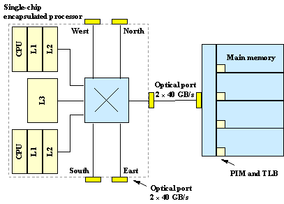
Fig. 9 – The encapsulated processor is a single CMOS chip with fiber-optic ports as the only means of external high-speed data communication. The processor consists of two CPUs with L1 and L2 cache connected by a crossbar switch. The crossbar connects to on-chip L3 cache and multiple high-speed fiber-optic ports. Each fiber-optic port is capable of sustaining 40 GB/s (320 Gb/s) data throughput in each direction and one such port is dedicated to local main memory. Main memory could be configured to have its own processors and TLB.The remaining optical ports are available for IO and scalable SAN interconnect. |
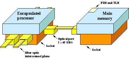
Fig. 10 – The encapsulated processor includes a socket that supplies DC current and ground. Incorporated into the socket are the physical optical ports, each of which provide 2 40 GB/s data bandwidth external to the encapsulated processor. One optical port is dedicated to local main memory. |
Scalability of the SAN is dependent on there being enough high-speed ports available for the network. In Fig. 9, the bisection bandwidth of an 8-port cross-bar switch latency by using pre-fetch. In addition to pre-fetch, there are other ways to use high bandwidth to keep the processor busy and increase overall system performance. One example is efficient multi-tasking. A high memory bandwidth allows cache to be quickly swapped between applications. Another example of the benefits of high memory bandwidth is the fact that block size of the L3 cache can be increased without incurring a significant L3 miss penalty.
While the advantages of high memory bandwidth are understood, conventional bus-based electrical solutions are performance limited. Today, a Pentium 4 processor with 1.7 GHz clock has an internal bandwidth of 13.6 GB/s, DDR SRAM has an internal burst bandwidth of at least this, but the system memory interface bandwidth is only 3.2 GB/s. The reason for the low memory bandwidth is easy to understand. For example, the periodically loaded 16 b-wide bus used in Rambus designs has a hard cut-off frequency of 1.5 GHz [10]. A 4-level electrical signaling scheme proposed by Rambus maintains a manageable bus clock frequency of 400 MHz at the expense of increased power dissipation, reduced noise tolerance, and some latency. The increased latency of two clock cycles is due to the requirement that multiple bits of data must be encoded and decoded per sampling period.
An alternative approach that delivers a low-latency solution and leverages the inherent advantages of fiber-optic technology is illustrated in Fig. 11. Here SDRAM is connected to a crossbar switch via 32 b-wide electrical point-to-point half-duplex links signaling at 2 Gb/s per pin. The crossbar is connected to the processor by a high bandwidth, low latency, WDM fiber-optic port. In this example, optically isolated communication from the microprocessor to latency by using pre-fetch.
In addition to pre-fetch, there are other ways to use high bandwidth to keep the processor busy and increase overall system performance. One example is efficient multi-tasking. A high memory bandwidth allows cache to be quickly swapped between applications. Another example of the benefits of high memory bandwidth is the fact that block size of the L3 cache can be increased without incurring a significant L3 miss penalty.
While the advantages of high memory bandwidth are understood, conventional bus-based electrical solutions are performance limited. Today, a Pentium 4 processor with 1.7 GHz clock has an internal bandwidth of 13.6 GB/s, DDR SRAM has an internal burst bandwidth of at least this, but the system memory interface bandwidth is only 3.2 GB/s. The reason for the low memory bandwidth is easy to understand. For example, the periodically loaded 16 b-wide bus used in Rambus designs has a hard cut-off frequency of 1.5 GHz [10]. A 4-level electrical signaling scheme proposed by Rambus maintains a manageable bus clock frequency of 400 MHz at the expense of increased power dissipation, reduced noise tolerance, and some latency. The increased latency of two clock cycles is due to the requirement that multiple bits of data must be encoded and decoded per sampling period.
An alternative approach that delivers a low-latency solution and leverages the inherent advantages of fiber-optic technology is illustrated in Fig. 11. Here SDRAM is connected to a crossbar switch via 32 b-wide electrical point-to-point half-duplex links signaling at 2 Gb/s per pin. The crossbar is connected to the processor by a high bandwidth, low latency, WDM fiber-optic port. In this example, optically isolated communication from the microprocessor to crossbar has approximately 3 ns latency and internal latency of the crossbar is near 3 ns. The total latency to request data from main memory and return it to the microprocessor of about 37 ns is dominated by the 25 ns core row-access latency of DRAM itself. As future memory designs improve on this value, the advantages of using a WDM fiber-optic port in combination with crossbar switches become more evident. The high bandwidth port consumes less power and less board area compared to any all-electrical alternative. In addition, memory can be scaled incurring minimal additional latency by adding crossbar switches.
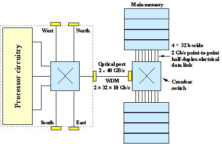
Fig. 11 – High bandwidth memory access via a WDM fiber-optic port capable of sustaining 40 GB/s (320 Gb/s) data throughput in each direction and a crossbar switch. Memory interfaces to the crossbar using half-duplex point-to-point electrical links signaling at 2 Gb/s. |
There are other reasons to maintain a focus on improving system interconnect bandwidth. As the Internet matures, bandwidth to a given node will dramatically increase. User applications will evolve to exploit IP and high-bandwidth connectivity. The influence of IP-centric applications in determining future system specification should not be underestimated. Optimizing system performance will require emphasizing high-speed IO.
In general, a high-bandwidth SAN also allows intelligence (and the associated power dissipation) to be distributed throughout the system. The processor and translation look-aside buffer in main memory is one such example.
High-performance encapsulated processors are serviced by high-bandwidth fiber-optic interconnects. In this way the encapsulated processor becomes a basic building-block for systems. This is the general-purpose processor of the future because the high-bandwidth fiber-optic ports enable a wide range of specialized system configurations.
Fiber-to-the-processor is a natural technology convergence point. It drives the evolution of the PC, workstation, server, mainframe, and router to one basic entity: the encapsulated processor.
The promise of fiber-optics is so great that it cannot be ignored. In fact, it is inevitable that, just as fiber-optics migrated from WAN to LAN and then to SAN, it will be embraced as the enabling technology to propel microprocessor platforms to the next level of performance. There are just too many good reasons for adopting the technology.
Fiber-to-the-processor is coming!
Author: Tony Levi is Professor of Electrical Engineering at the University of Southern California and serves on the technical advisory board of Primarion Inc. and Archway Inc.
References
[1] G. E. Moore, Electronics 38, 114-117 (1965). Also reprinted in Proc. IEEE 86, 82-85 (1998).
[2] Data from the Intel web site,
http://www.intel.com/research/silicon/mooreslaw.htm
[3] Intel data sheets.
[4] B. Raghavan and A. F. J. Levi, unpublished.
[5] A. F. J. Levi, Proc. IEEE 88, 750-757 (2000).
[6] http://www.oiforum.com/
[7] Now an Agilent Technologies product number HFBR 712BP. Also see http://www.agilent.com/
[8] B. Madhavan and A. F. J. Levi, Electron. Lett. 34, 178-179 (1998).
[9] P. Wijetunga and A. F. J. Levi, unpublished.
[10] http://www.rambus.com/developer/
application_briefs.html
Other articles on FTTP:
