Introduction
Devices, components, and sub-systems with new capabilities must be created to meet future system engineering needs. The large number of degrees of freedom associated with quantum systems suggests this is an ideal area within which to search for new functional behavior. The states of electrons and photons can be described in combinations that include coherent superposition. In addition, there are atomic internal degrees of freedom. Among the latter are orbital degrees of freedom that can result in bonding and spin degrees of freedom that can give rise to magnetism.
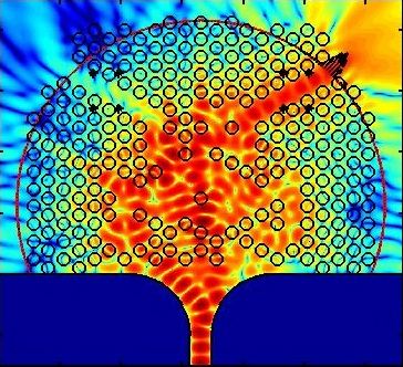
The challenge of how to explore and discover useful functionalities in a vast configuration space may be addressed using machine-based searches. Our current research effort is focused in a few specific directions such as creating an optimized semiconductor optical modulator, controlling scattering of electromagnetic radiation off aperiodic dielectric structures, and controlling nanometal-light interaction. In this on-going proof-of-principle study, it is already clear that such an approach to device design is going to be worthwhile. The underlying reason is that exposing more degrees of freedom tends to increase accessibility to functionality.
The device synthesis methodology we use exploits advances in applied mathematics, computer science, development of realistic physical models, available compute power, nanoscience, and device engineering. Today, our interdisciplinary research effort involves collaborations with the Physics, Mathematics, and Electrical Engineering departments at USC as well as researchers at MIT and NYU.
 |
 |
 |
 |
Adaptive quantum design for device synthesis:
The design of both photonic and electronic devices have evolved over many years in an essentially ad-hoc way. There is, for example, a long history of laser diode and photodiode design that incrementally builds on previous designs and concepts. The same is true for transistor design. A very unfortunate consequence of adopting such an incremental ad-hoc design approach is the emergence and continued use of non-optimize designs. We believe that there is an opportunity to reverse these trends by creating a new strategy in which device function and fabrication process are integrated. Such an integrated product process design harnesses a combination of modern compute power, adaptive algorithms, and realistic physical models, to seek robust, manufacturable designs for components that meet previously unobtainable system specifications. Using these new device synthesis techniques it will be possible to break the cycle of incremental ad-hoc design methods and discover completely new functionality for both photonic and electronic devices.