EE 506 – Semiconductor Physics
30822R
Days Mon, Wed: Time 9:00 am – 10:50 am
Location THH 115 (Taper Hall)
TA is NA, meeting NA
Web sites:
http://classes.usc.edu/term-20241/classes/ee
First day of classes Monday January 8, 2024
Last day of classes Wednesday April 24, 2024
Study Days: Saturday, April 27 – Tuesday, April 30, 2024
Final Exam: TTH 115, Friday, May 3, 2024, 8.00am – 10.00am
Office Hours: Tuesdays, KAP132, 2:00 pm – 4:00 pm or by appointment
Semiconductor electronic devices manufactured on silicon substrates can now be found in, and contribute to, every aspect of modern life. A pinnacle of human achievement is creation of electronic grade materials and their precision manufacturing into electrical circuits with control at the nanometer scale. This capability, a direct result of curiosity-driven science and application-inspired engineering, has enabled contemporary electronics, circuits that contain billions of transistors, computing, communication, and access to opportunities in the cyber world. Non-silicon semiconductor technologies are also making contributions and helping create new system capabilities.
This course will explore the physics that underpins the behavior and properties of semiconductors and their device applications. It aims to provide a framework and understanding that can be used to develop a methodology for creation of new combinations of materials, device geometries, and device functionality.
Prerequisite: Understanding to approximately the level of either MS/EE 501 Solid State Physics or EE 539 Quantum Mechanics
Instructor: A.F.J. Levi
Suggested background reading: Essential Electron Transport for Device Physics, A.F.J. Levi, AIP, ISBN: 978-0-7354-2158-5.
Grading: Homework 20%
Midterm Exam 30%
Final Exam 50%
Essential ideas:
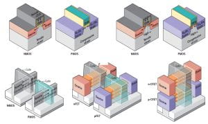
Lecture 1: Motivation. Semiconductors and electronics. Evolution of materials and geometries used in creation of transistors:


Lecture 2: Atom “shape” in solid materials determines crystal structure. The critical role of quantized electron orbitals. The hydrogen atom. The Pauli exclusion principle and the periodic table of elements. Hybridization.
Lecture 3: Bonds. The hydrogen molecule ion. The hydrogen molecule covalent bond using valence bond and molecular orbital description. The ionic bond.
Lecture 4: Crystal structure. Crystal systems in three-dimensions. The reciprocal lattice. Nonequilibrium materials and disordered materials. Isotropic materials with linear local response. Bloch’s theorem. Localized Wannier functions. Crystal momentum and electron effective mass.
Lecture 5: The generalized Kronig-Penney model and complex band structure.
Lecture 6: Introduction to the tight-binding method. A single s-band in a one-dimensional lattice. Density of electron states. A one-dimensional lattice with a two-atom basis, the example of trans-polyacetylene. Complex band structure in the tight-binding approximation. Single electron wave packet tunneling and complex band structure.
Lecture 7: Graphene lattice. Carbon sp2 hybridization and bonding. Graphene band structure calculated using the tight-binding method. Electron transport in graphene.
Lecture 8: Band structure: Tight-binding method in three dimensions based on the paper by Vogl et al., (1983). The band structure of III-V and group-IV semiconductors.
Lecture 9: Band structure: Kane’s k.p method. Hartree self-consistent solution to Schrodinger and Poisson equation, Hartree-Fock, and density functional theory.
Lecture 10: Doping electrons and holes. The semiconductor heterostructure. The gap state model. Substitutional doping of electrons and holes. Metallic behavior and rs. Density of electron states at band extremum. Fermi particle statistics, few-electron fermi-particle statistics, the Fermi-Dirac distribution. The Bose-Einstein distribution. The chemical potential. The electron propagation matrix. Current-voltage characteristic of a semiconductor heterostructure tunnel diode. Calculation of the semiconductor heterostructure tunnel diode current in the depletion approximation.
Lecture 11: Electron transmission in the presence of inelastic scattering. Inelastic electron tunneling spectroscopy.
Lecture 12: Lattice vibrations. The damped driven oscillator. Noise, fluctuation-dissipation theorem, and diffusion. Einstein relation.
Lecture 13: Optimal semiconductor device design. Cost function, distance measure, noise in data, regression. The heterostructure tunnel diode forward model. The adjoint method.
Lecture 14: Machine generated, non-intuitive, optimal semiconductor heterostructure tunnel diode device design for user specified current-voltage characteristics.
Lecture 15: Review.
Lecture 16: Current. Charge transport in semiconductor devices. Electron transport in semiconductors. Electron wave packet dynamics at a tunnel barrier.
Lecture 17: Bloch oscillations. Material parameters contributing to current. Velocity field characteristics and electron transfer to subsidiary minima. The Gunn diode oscillator. Ballistic transport.
Lecture 18: The Boltzmann transport equation. Evolution of the distribution function with time. The scattering term. Relaxation time approximation. Conductivity. The diffusion term.
Lecture 19: Mean free path and scattering time from mobility. Mean free path and scattering time in 2DEG. Electron optics in the 2DEG. Diffusion in devices. Diffusion and recombination of minority carriers. The metal-semiconductor Schottky barrier. Depletion width. Thermionic emission. Capacitance as a function of voltage bias. Single-crystal nickel-silicide silicon Schottky diode and metal-induced gap states.
Lecture 20-21: Electron scattering in semiconductors. The electron-phonon interaction. The Frohlich interaction. The longitudinal polar-optic phonon scattering rate. The LO phonon scattering rate in the conduction band of GaAs. Energy and momentum conservation. Electron scattering rate from linear dielectric response. Scattering rates and fluctuation dissipation.
Lecture 22-23: Elastic scattering from ionized impurities. The screened coulomb potential. Elastic scattering of electron from ionized impurities in GaAs. Correlation effects due to spatial position of dopant atoms. estimating mean free path and mobility. Calculating the screened potential and dielectric function in wave vector space. Comparison between Thomas-Fermi screening and RPA.
Lecture 24-25: RPA and inelastic scattering of majority carriers in n-type semiconductors. Inelastic scattering of minority carriers in p-type semiconductors.
Lecture 26-27: Review